- 您现在的位置:买卖IC网 > Sheet目录308 > ADUM5402WCRWZ (Analog Devices Inc)IC ISOLATOR 4CH DCDC CONV 16SOIC
ADuM5401W/ADuM5402W/ADuM5403W
Data Sheet
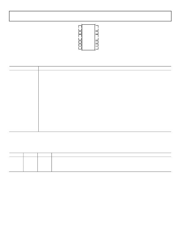
V DD1 1
GND 1 2
16
15
V ISO
GND ISO
V IA 3
ADuM5403W
14
V OA
V OB 4
TOP VIEW
13 V IB
V OC 5
(Not to Scale) 12 V IC
V OD 6
RC OUT 7
GND 1 8
11
10
9
V ID
V SEL
GND ISO
Figure 8. ADuM5403W Pin Configuration
Table 23. ADuM5403W Pin Function Descriptions
Pin No.
1
2, 8
3
4
5
6
7
9, 15
10
11
12
13
14
16
Mnemonic
V DD1
GND 1
V IA
V OB
V OC
V OD
RC OUT
GND ISO
V SEL
V ID
V IC
V IB
V OA
V ISO
Description
Primary Supply Voltage, 3.0 V to 5.5 V.
Ground Reference for the Primary Side of the Isolator. Pin 2 and Pin 8 are internally connected to each other, and it
is recommended that both pins be connected to a common ground.
Logic Input A.
Logic Output B.
Logic Output C.
Logic Output D.
Regulation Control Output. This pin is connected to the RC IN pin of a slave iso Power device to allow the ADuM5403W
to control the regulation of the slave device.
Ground Reference for the Secondary Side of the Isolator. Pin 9 and Pin 15 are internally connected to each other,
and it is recommended that both pins be connected to a common ground.
Output Voltage Selection. When V SEL = V ISO , the V ISO setpoint is 5.0 V. When V SEL = GND ISO , the V ISO setpoint is 3.3 V.
Logic Input D.
Logic Input C.
Logic Input B.
Logic Output A.
Secondary Supply Voltage Output for External Loads: 3.3 V (V SEL = GND ISO ) or 5.0 V (V SEL = V ISO ).
TRUTH TABLE
Table 24. T ruth Table (Positive Logic)
V SEL
High
Low
Low
High
RC OUT 1
PWM
PWM
PWM
PWM
V DD1 (V)
5
5
3.3
3.3
V ISO (V)
5
3.3
3.3
5
Notes
Master mode, normal operation
Master mode, normal operation
Master mode, normal operation
This supply configuration is not recommended due to extremely poor efficiency
1
PWM refers to the regulation control signal. This signal is derived from the secondary side regulator and can be used to control other iso Power devices.
Rev. D | Page 14 of 24
发布紧急采购,3分钟左右您将得到回复。
相关PDF资料
ADUM5404CRWZ
IC ISOLATOR 4CH DCDC CONV 16SOIC
ADUM6132ARWZ-RL
IC GATE DRIVER ISOLATED 16-SOIC
ADUM6201CRIZ
ISOLATED DC-DC CONV 2CH 16SOIC
ADUM6404ARWZ
IC ISOLATOR 4CH DCDC CONV 16SOIC
ADUM7241CRZ-RL7
ISOLATOR DGTL 1KVRMS 2CH 8SOIC
ADUM7440CRQZ-RL7
IC DIGITAL ISOLATOR 4CH 16QSOP
ADUM7510BRQZ
IC DGTL ISOLATOR 5CH 16QSOP
ADZS-21364-EZLITE
KIT EVAL EZ LITE ADDS-21364
相关代理商/技术参数
ADUM5402WCRWZ-1
功能描述:ISOLATOR 4CH DCDC CONV 16SOIC RoHS:是 类别:隔离器 >> 数字隔离器 系列:* 产品培训模块:IsoLoop® Isolator 标准包装:50 系列:IsoLoop® 输入 - 1 侧/2 侧:5/0 通道数:5 电源电压:3 V ~ 5.5 V 电压 - 隔离:2500Vrms 数据速率:110Mbps 传输延迟:12ns 输出类型:CMOS 封装/外壳:16-SOIC(0.154",3.90mm 宽) 供应商设备封装:16-SOIC N 包装:管件 工作温度:-40°C ~ 85°C 其它名称:390-1053-5
ADUM5402WCRWZ-1RL
功能描述:ISOLATOR 4CH DCDC CONV 16SOIC RoHS:是 类别:隔离器 >> 数字隔离器 系列:* 产品培训模块:IsoLoop® Isolator 标准包装:50 系列:IsoLoop® 输入 - 1 侧/2 侧:5/0 通道数:5 电源电压:3 V ~ 5.5 V 电压 - 隔离:2500Vrms 数据速率:110Mbps 传输延迟:12ns 输出类型:CMOS 封装/外壳:16-SOIC(0.154",3.90mm 宽) 供应商设备封装:16-SOIC N 包装:管件 工作温度:-40°C ~ 85°C 其它名称:390-1053-5
ADUM5402WCRWZ-RL
功能描述:IC ISOLATOR 4CH DCDC CONV 16SOIC RoHS:是 类别:隔离器 >> 数字隔离器 系列:IsoPower®, iCoupler® 产品培训模块:IsoLoop® Isolator 标准包装:50 系列:IsoLoop® 输入 - 1 侧/2 侧:5/0 通道数:5 电源电压:3 V ~ 5.5 V 电压 - 隔离:2500Vrms 数据速率:110Mbps 传输延迟:12ns 输出类型:CMOS 封装/外壳:16-SOIC(0.154",3.90mm 宽) 供应商设备封装:16-SOIC N 包装:管件 工作温度:-40°C ~ 85°C 其它名称:390-1053-5
ADUM5402WXRWZ
功能描述:DGTL ISO 2.5KV GEN PURP 16SOIC 制造商:analog devices inc. 系列:* 零件状态:上次购买时间 标准包装:1
ADUM5403
制造商:AD 制造商全称:Analog Devices 功能描述:Quad-Channel, 2.5 kV Isolators with Integrated DC-to-DC Converter
ADUM5403ARWZ
功能描述:IC ISOLATOR 4CH DCDC CONV 16SOIC RoHS:是 类别:隔离器 >> 数字隔离器 系列:IsoPower®, iCoupler® 标准包装:66 系列:iCoupler® 输入 - 1 侧/2 侧:2/2 通道数:4 电源电压:3.3V,5V 电压 - 隔离:2500Vrms 数据速率:25Mbps 传输延迟:60ns 输出类型:逻辑 封装/外壳:20-SSOP(0.209",5.30mm 宽) 供应商设备封装:20-SSOP 包装:管件 工作温度:-40°C ~ 105°C
ADUM5403ARWZ1
制造商:AD 制造商全称:Analog Devices 功能描述:Quad-Channel Isolators with Integrated DC-to-DC Converter
ADUM5403ARWZ2
制造商:AD 制造商全称:Analog Devices 功能描述:Quad-Channel Isolators with Integrated DC-to-DC Converter
